


Gerber2PNG — Making PCB Milling at FabLabs Simpler
If you’ve ever been through a FabAcademy cycle or spent time at a FabLab, you’ll know the PCB milling workflow is both magical and maddening. Designing circuits is fun, but the moment you try to get them onto a board with a milling machine, you hit a wall.
Why we built this
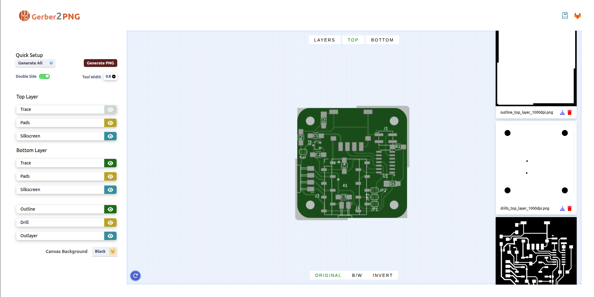
In Fab Labs worldwide, PCB milling is often done with Fab Modules (FabMods), a tool originally developed at MIT. But here’s the catch: FabMods doesn’t accept Gerber files directly — it needs black & white PNGs for each layer:
That means:
- A monochrome PNG for the copper traces
- Another for drill holes
- And one more for the board outline (edge cuts)
Until now, this meant makers had to manually convert Gerbers using Photoshop, GIMP, or Photopea — repeating the process layer by layer. It was slow, error-prone, and intimidating for beginners.
That’s where Gerber2PNG comes in.
What is Gerber2PNG?
Gerber2PNG is a browser-based tool that takes raw Gerber files from popular EDA tools like KiCad, Eagle, Altium, Fusion 360, EasyEDA, and Proteus, and instantly transforms them into clean, monochrome PNGs ready for FabMods or other CAM tools. The process is simple: upload your files, select whether it’s a single or double-sided PCB, and generate layer-specific PNGs with a single click.
What once required hours of manual work in software like Photoshop or GIMP is now fully automated. The tool produces separate outputs for traces, drill holes, and edge cuts while keeping everything properly aligned so that nothing shifts unexpectedly when you start milling. Its interface was designed to be straightforward and beginner-friendly, ensuring that even first-time users can prepare fabrication-ready files without struggling through complex settings.
For single-sided PCBs, this already saves hours of frustration. But we knew the real pain point was still lurking: double-sided boards.
The double-sided nightmare
Creating two-sided PCBs has always been one of the hardest parts of FabLab PCB milling. Even if you managed to export both layers correctly, flipping the board and aligning it with the original cutout was a nightmare. Traditionally, FabLabs relied on improvised tricks: drilling alignment holes, eyeballing offsets, or trial-and-error with scraps of copper board. Beginners dreaded it. Experts found it unreliable.
Gerber2PNG solves this problem by baking alignment directly into the conversion process. When you select Double Side mode, the tool automatically adds alignment notches to the first edge cut. These notches, precisely the width of your milling bit, are placed at two opposite corners of the board. When it’s time to flip the PCB, it slots perfectly back into the same position — no guesswork, no misalignment, just tight-fit precision.
How it works behind the scenes
Even though the interface is beginner-friendly, the backend does a fair bit of heavy lifting:
Parsing Gerbers — The tool reads copper, drill, and outline layers. Under the hood, we use the
gerber-to-svgnpm library to convert Gerber files into a single, complete SVG containing all the layers.SVG manipulation — Once the SVG is generated, we programmatically manipulate it to match our specific needs, like isolating layers, adjusting dimensions, or modifying paths.
Canvas rendering — The manipulated SVG is then drawn onto a virtual canvas, allowing us to render the layers exactly as needed.
Rasterization & PNG output — From the canvas, we generate clean, high-contrast PNG images, ready for FabMods.
Layer processing & alignment tweaks — In double-sided mode, edge cuts are adjusted with protrusions for precise registration, ensuring perfect alignment when flipping the board.
From the user’s perspective: drag, drop, done. From the machine’s perspective: perfect inputs, every time.
Best practices & troubleshooting
To get reliable results, the following must be taken care of:
| What can go wrong | Why it happens | What to do |
|---|---|---|
| Blank PNG / no traces visible | Gerber export had wrong layers, missing copper, origin wrong, or invalid format | Double-check export settings; use viewer to verify Gerber file first |
| Misaligned top and bottom layers (for double-sided) | Mirroring or origin not consistent among layers | Ensure origin and axis settings are same; align via auxiliary origin point etc. |
| Large file size or slow conversion | Very fine details, many polygons, very high resolution requested | Try lowering resolution; simplify polygons; only include needed layers |
| Unsupported Gerber flavor / commands | Some exports use odd/non-standard variations | Use standard Gerber (RS-274X etc.) if possible; test with small sample |
Origins & Credits
Gerber2PNG was born at Super FabLab Kerala, developed by Muhammed Midlaj N and Saheen Palayi, with guidance from Jogin Francis and Yadu Sharon.
It was shaped by the day-to-day frustrations of FabAcademy students and our team — people who just wanted their boards fabricated without wasting time on file conversions.
We open-sourced it under the MIT license, because this problem isn’t unique to one lab. Every FabLab can benefit from smoother, faster PCB prep.
The tool is publicly accessible at gerber2png.fablabkerala.in, so anyone can use it to streamline their PCB workflow.
Final Thoughts
Fab Labs are about accessibility. By removing tedious, error-prone steps, Gerber2PNG helps more people succeed in making real hardware.
- Students in Fab Academy can mill PCBs without ever opening Photoshop.
- Beginners get their boards right on the first try.
- Experts save time and avoid silly mistakes.
It’s a small tool — but it smooths a critical step in the global FabLab workflow.